Applications
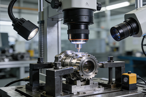
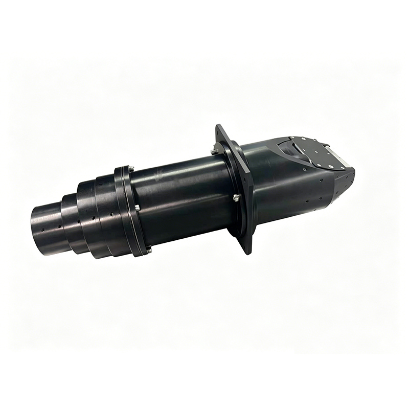
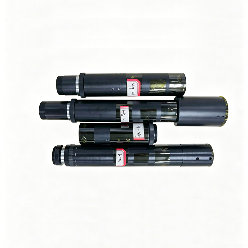
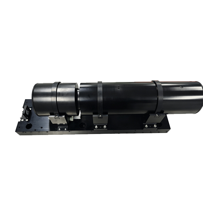
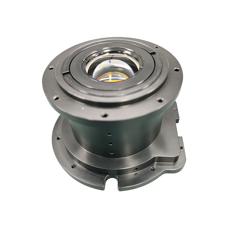
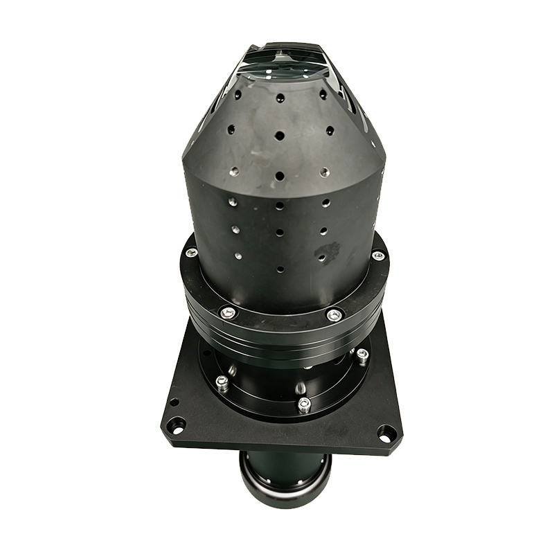
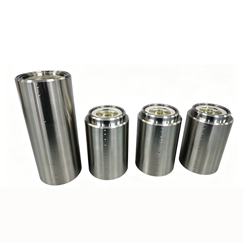
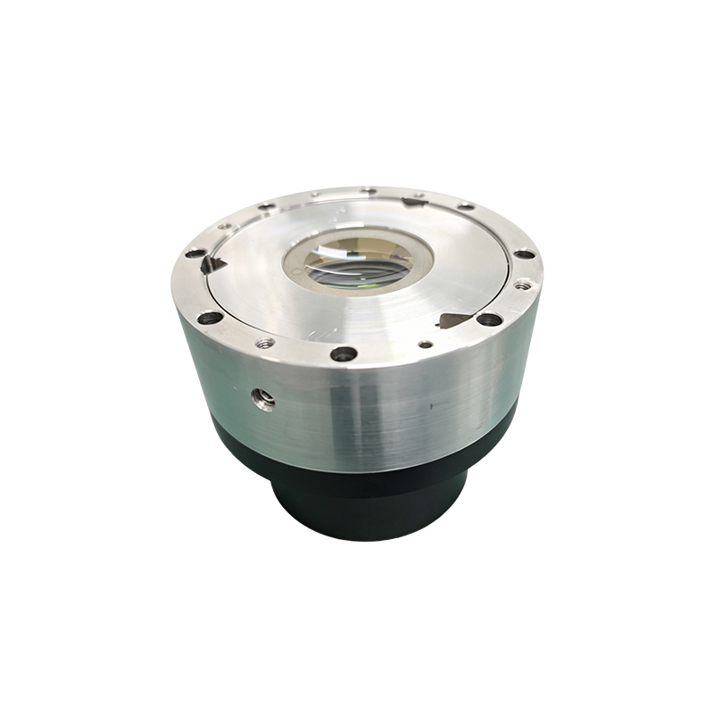
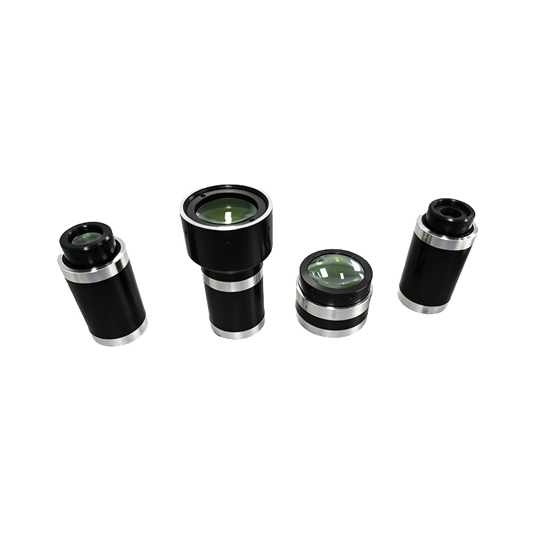
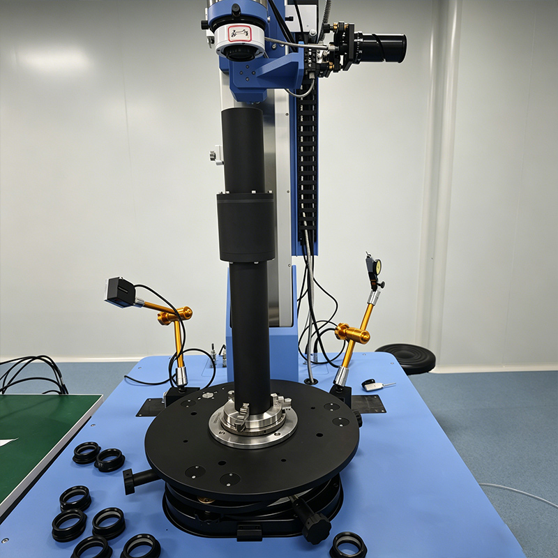
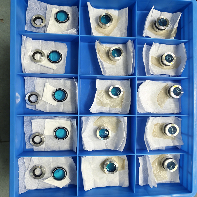
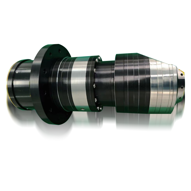
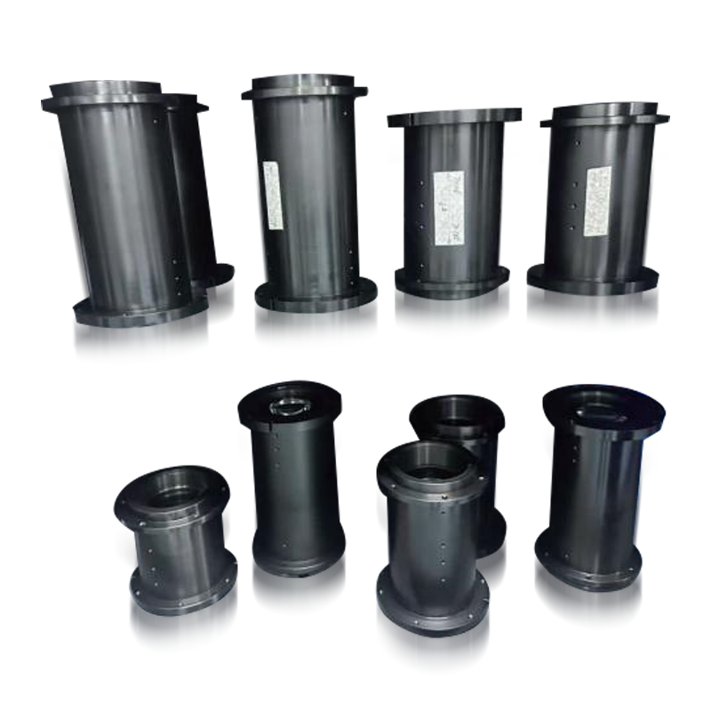
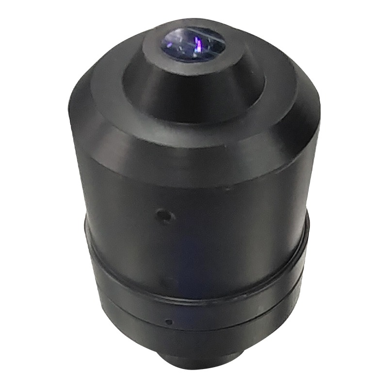
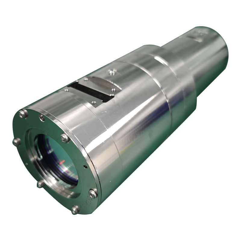
Industrial imaging lenses support dimensional measurement, surface inspection and defect detection throughout production and quality control. Optical design is matched to the camera, working distance, field of view and inspection environment.
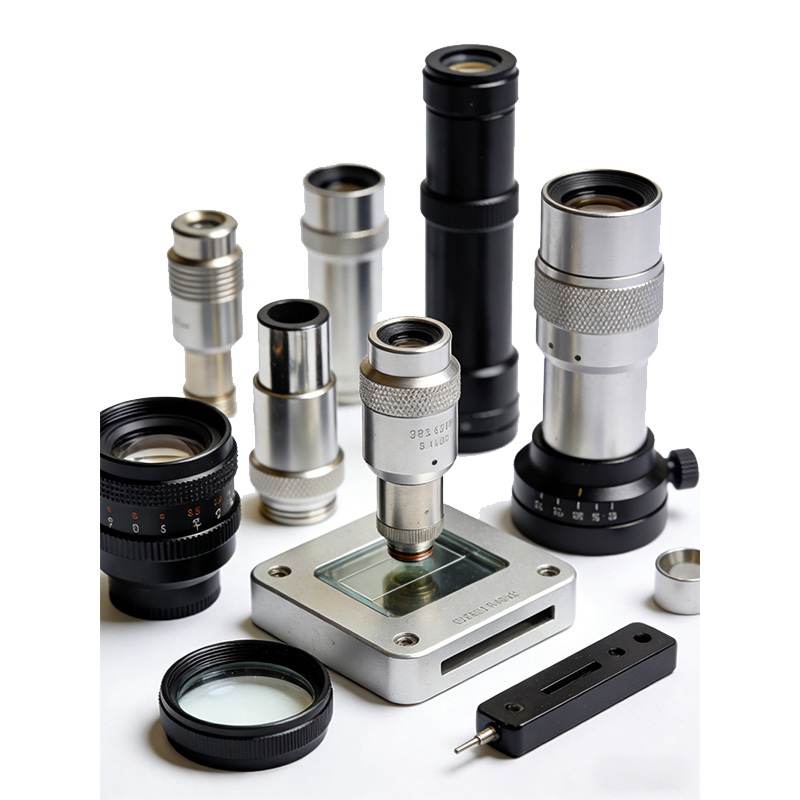
Telecentric and microscope optics are used to inspect precision components for dimensional variation, scratches, cracks and burrs. Other applications include wafer inspection, semiconductor packaging and printed-circuit-board inspection.
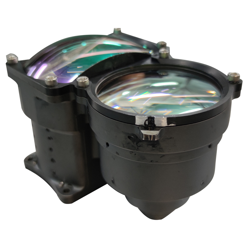
Wide-field and high-speed imaging supports packaging and print inspection, including registration errors, missing print and surface damage. Custom focal lengths and apertures help integrate the optical system with automated, continuous inspection equipment.