Applications
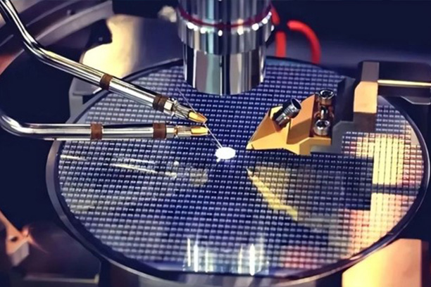
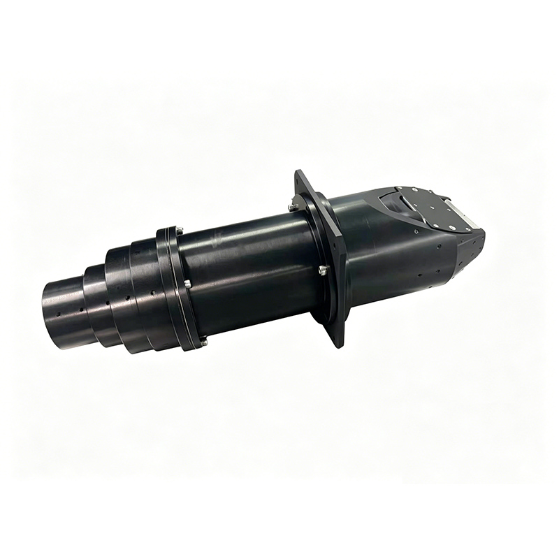
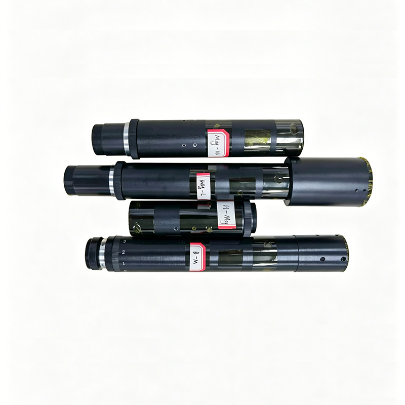
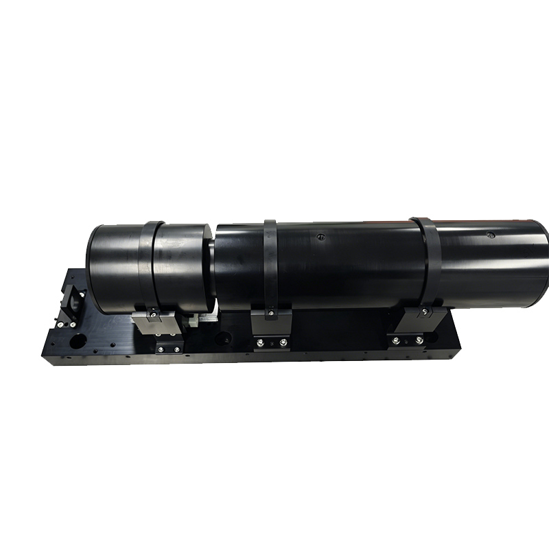
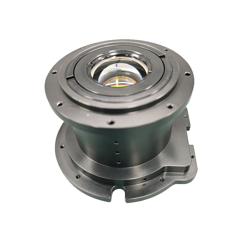
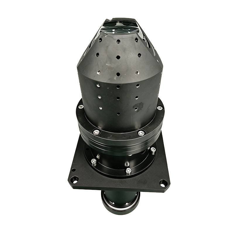
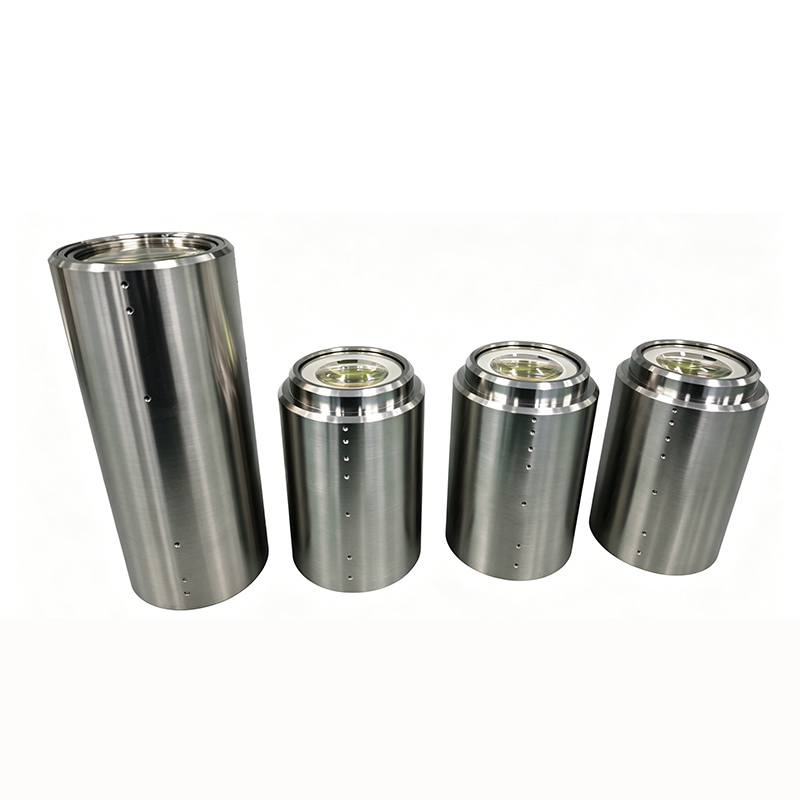
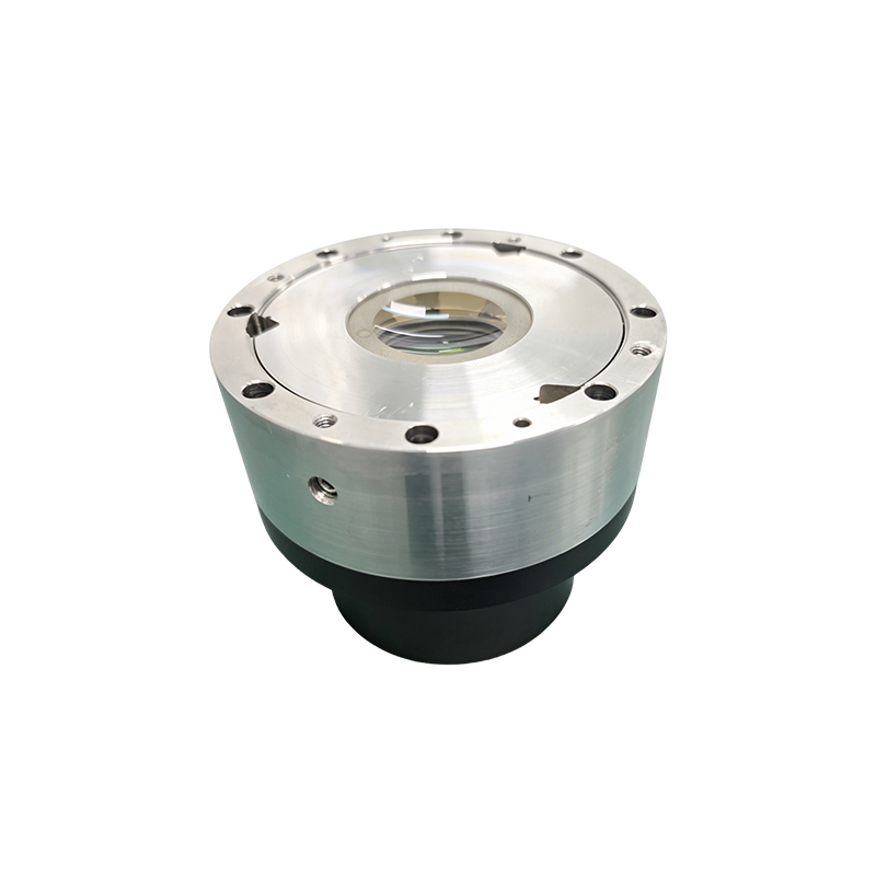
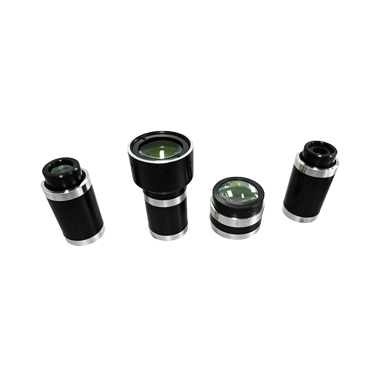
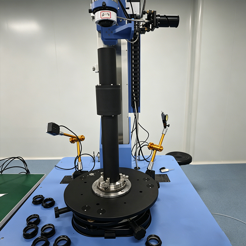
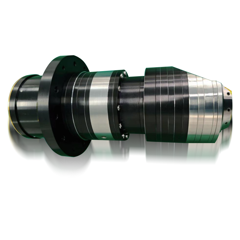
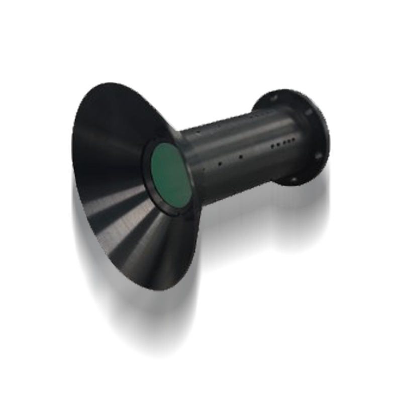
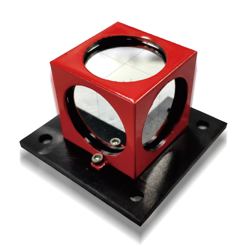
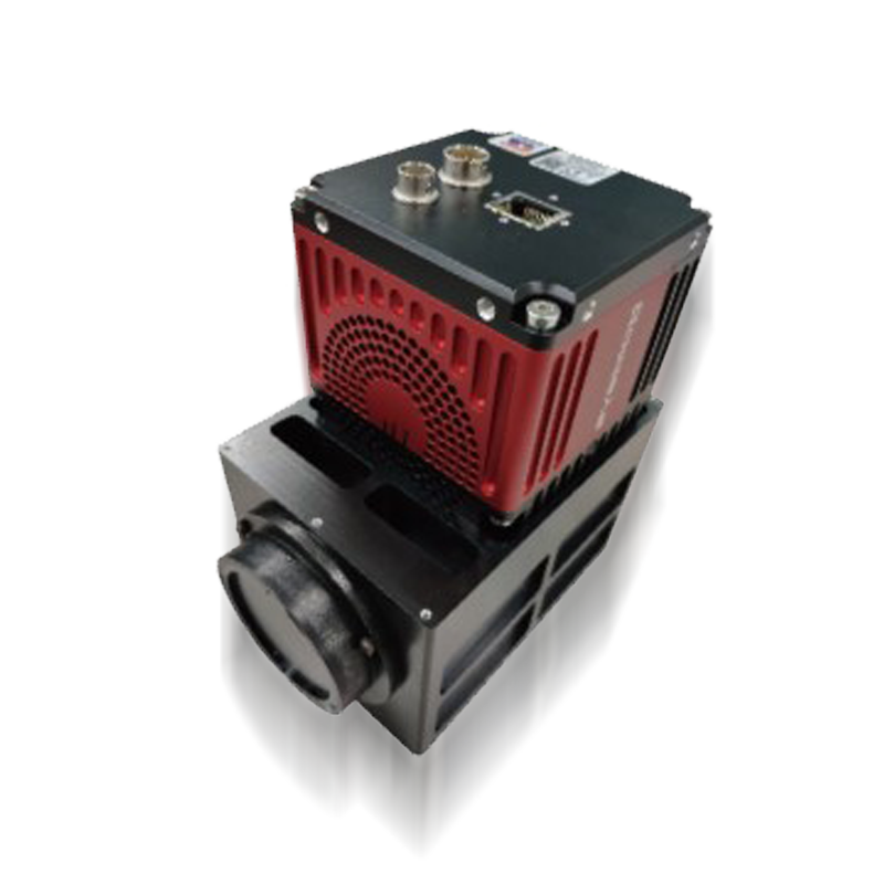
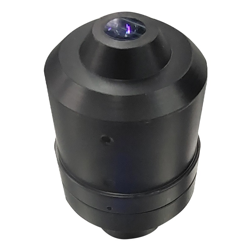
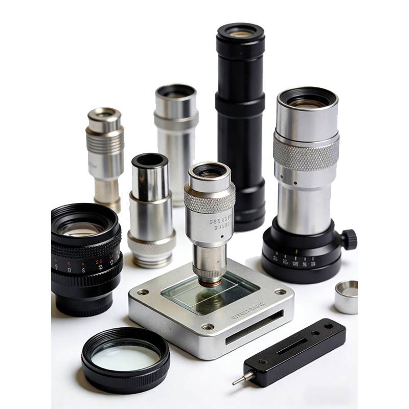
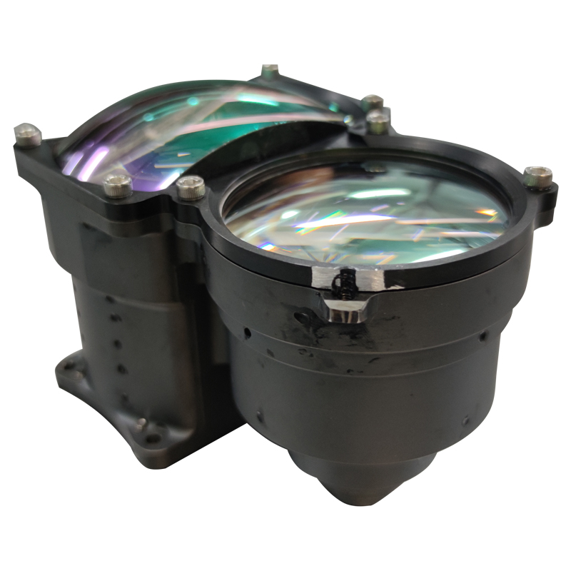
Semiconductor inspection relies on stable, high-resolution optics throughout wafer processing, packaging and testing. Microscope and telecentric lens designs support surface-defect inspection, pattern alignment and optical metrology.
Packaging applications include lead alignment, package inspection and positioning a chip relative to its substrate. Magnified imaging can also assist inspection of solder joints, circuit patterns and visible damage.
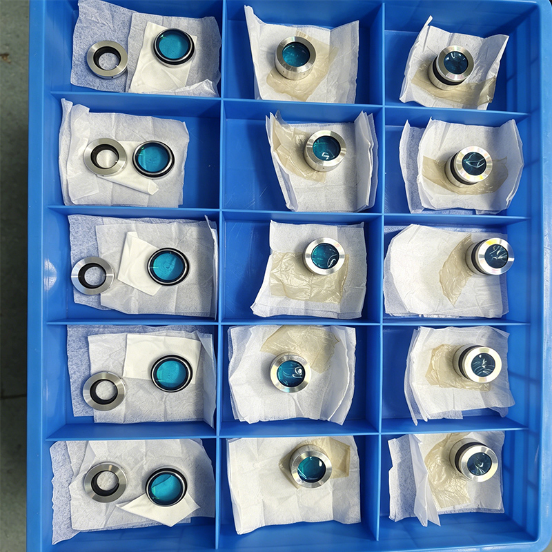
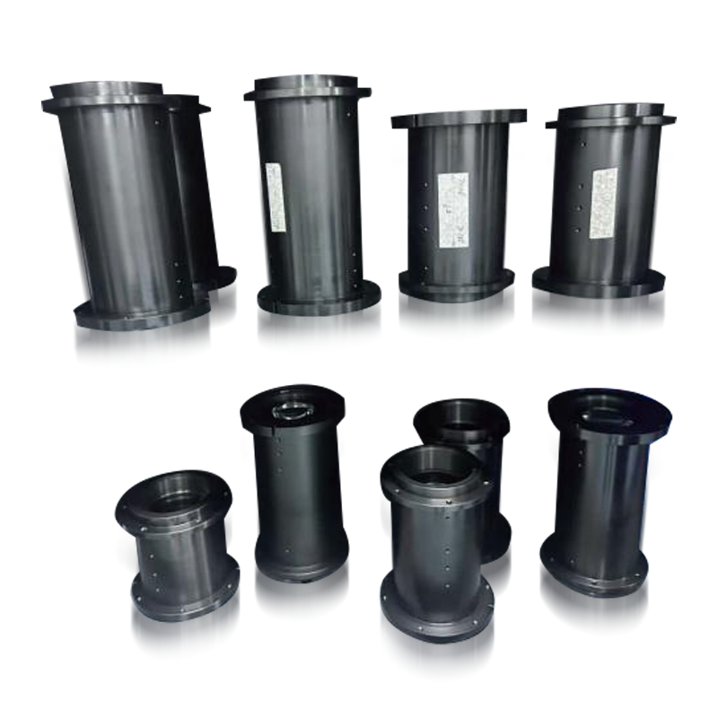
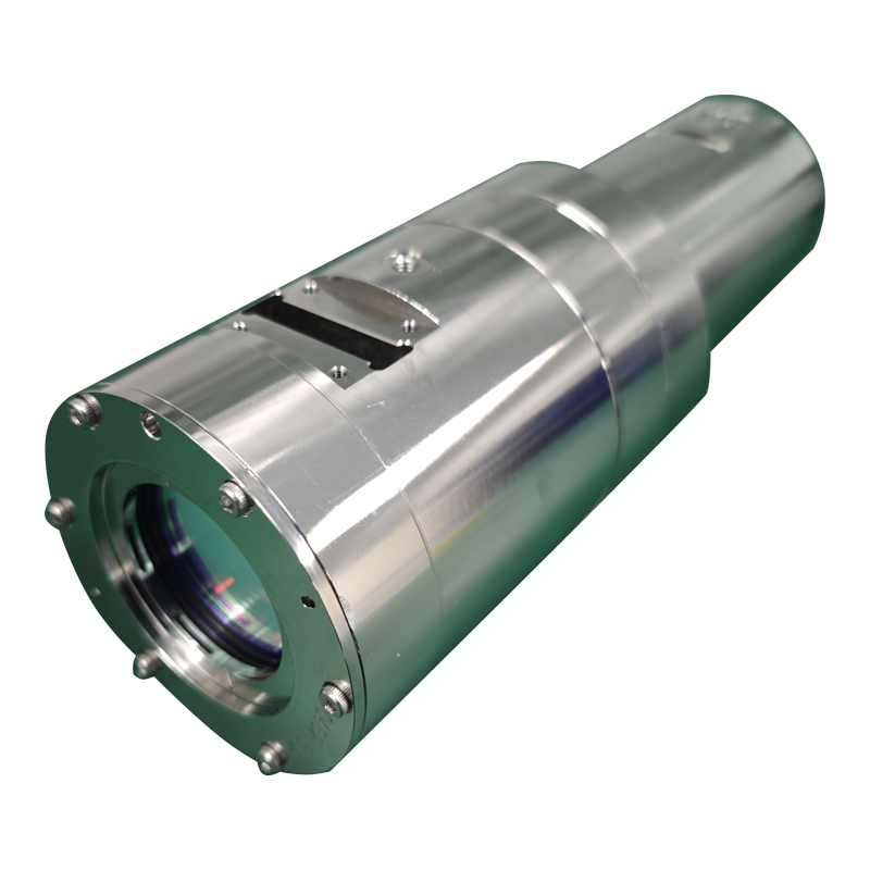
Optical specifications are selected for wafer dimensions, sensor format, required field of view and resolution. Mechanical integration, focus stability and the operating environment are considered as part of the system design.